
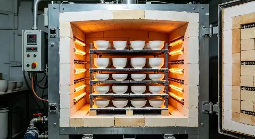
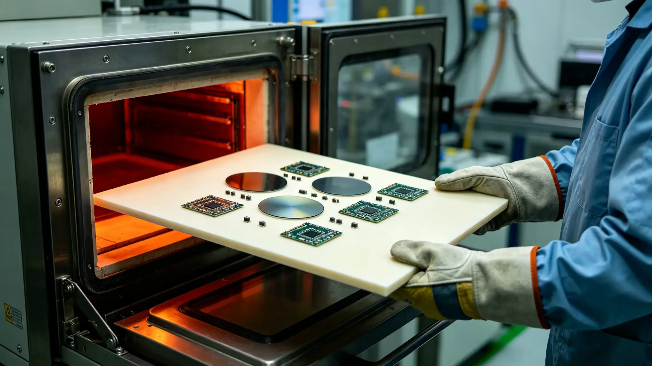
Overview of the development and analysis of sintering technologies for advanced ceramics and ceramic substrates
The evolution towards advanced sintering is driven by the demands of modern applications. In aerospace, components like missile nose cones require exceptional thermal stability and mechanical strength -1. In electronics, multi-layer ceramic substrates (e.g., for 5G RF front-end modules) demand precise co-firing of conductive metals and ceramics without deformation or interfacial reactions -2. These requirements have catalyzed the development of innovative sintering paradigms that offer superior microstructural control, reduced energy input, and compatibility with novel material systems.
2. Advanced Sintering Methodologies
2.1 Electric Field-Assisted Sintering Techniques
Electric field-assisted sintering, particularly Flash Sintering (FS), has emerged as a promising rapid sintering technique. It utilizes Joule heating generated by an electric field applied directly to the ceramic sample, enabling ultra-fast heating rates on the order of 10⁴ °C/min and achieving densification in mere seconds -5. However, a major bottleneck has been its tendency to cause macro-cracks in larger samples due to thermal stresses from the ultra-fast heating.
A significant breakthrough, Controlled Electric Field Sintering (ECS), has recently been developed to address this. As illustrated in the flowchart, ECS employs a controlled current profile to deliberately slow the heating rate to a range of 100–300 °C/min -5. This controlled ramp rate allows for more uniform heat distribution, effectively suppressing internal cracking. This method has successfully produced large, macro-crack-free bulk samples (up to 30 mm) of various materials, including MAX phases (e.g., Ti₃SiC₂), ultra-high-temperature ceramics (e.g., ZrB₂-SiC), and refractory metals, with relative densities exceeding 99% -5.
Furthermore, ECS has proven to be a powerful tool for revealing athermal effects—effects induced directly by the electric current, separate from Joule heat. In WC-6Co, the current was found to promote the formation of a Co₃W₃C phase, accelerating densification and improving mechanical properties. In Molybdenum (Mo), the current suppressed the formation of Mo₂C and promoted a more uniform distribution of low-angle grain boundaries, effectively doubling the flexural strength compared to conventional sintering -5.
2.2 Integration with Additive Manufacturing (3D Printing)
The synergy between advanced sintering and additive manufacturing (AM) is opening new frontiers for fabricating complex ceramic components that are impossible to achieve with traditional methods. The process typically involves Direct Ink Writing (DIW) or other 3D printing techniques to create a green body with a designed architecture, followed by a debinding and sintering step.
A prime example is the fabrication of Li₄SiO₄-Li₂TiO₃ dual-phase tritium breeder ceramics for nuclear fusion applications. Researchers combined 3D printing with precursor reaction sintering to create microspheres and complex triply periodic minimum surface (TPMS) structures -3. This approach overcame the limitations of traditional methods, such as poor controllability and low density. Through orthogonal experiment optimization, they achieved microspheres with a high relative density of 92.9% and a crushing load of 98.7 N, alongside TPMS-structured units with enhanced mechanical properties -3.
From a modeling perspective, mesoscopic simulations have become crucial for understanding sintering in AM components. These models simulate the evolution of surface roughness, grain growth, and pore shrinkage during the sintering of DIW-produced filaments. Studies have shown that a bimodal particle size distribution (PSD) in the ink enhances pore shrinkage kinetics but may also lead to highly eccentric pores, which could be detrimental to mechanical strength -9. This insight allows for the optimization of ink formulation and process parameters to achieve the desired final microstructure.
2.3 Low-Temperature Co-fired Ceramics (LTCC) and Sintering Aids
LTCC technology is a cornerstone of modern electronic packaging, enabling the integration of multi-layer circuits and embedded passive components. The core requirement is sintering the ceramic substrate below the melting point of high-conductivity electrode metals like silver (~961 °C), typically at 850–900 °C -2-8.
Achieving this requires two primary strategies:
-
Sintering Aids: Low-melting-point additives are introduced to promote liquid-phase sintering. For instance, in lead-free piezoelectric BNT-BT-KNN ceramics, adding 1.5 wt% B₂O₃ acted as a flux, allowing sintering at reduced temperatures while achieving a high piezoelectric coefficient (d₃₃ = 210 pC/N) -7. Similarly, in Li₂.₇₅MgTiO₄F₀.₇₅ microwave dielectric ceramics, unreacted LiF served as a sintering aid, enabling densification at 850 °C -8.
-
Precise Process Control: The LTCC manufacturing process involves several critical steps. It starts with the preparation of "green tape" from ceramic powder. Laser drilling (using picosecond/UV lasers) creates micro-vias with high aperture consistency (±3 μm), which are then filled with conductive paste (e.g., Ag, Cu) via micro-hole injection to form vertical interconnects -6. Multiple layers are then aligned (requiring sub-micron accuracy), laminated, and subjected to co-firing in an inert atmosphere at 850-900 °C -2-6. The major challenges here include controlling shrinkage and camber, which require precise matching of the thermal expansion coefficients of the ceramic and metal (difference ≤ 1 ppm/°C) to prevent delamination or warping -2.
3. Comparative Analysis & Future Outlook
The table below summarizes the key characteristics of the discussed sintering techniques.
| Sintering Technique | Typical Heating Rate | Key Advantage | Primary Challenge | Example Application |
|---|---|---|---|---|
| Traditional | ~30 °C/min -5 | Simplicity, scalability | High energy, long cycle | Conventional structural ceramics |
| Flash Sintering (FS) | ~10⁴ °C/min -5 | Ultra-fast, energy-efficient | Cracking in large samples | Lab-scale R&D |
| Control Electric Field (ECS) | 100-300 °C/min -5 | Crack-free bulk parts, athermal effects | Process complexity & control | High-performance bulk ceramics (MAX phases, WC-Co) -5 |
| Reaction Sintering + AM | Programmable | Geometrical freedom, high density | Defect control (eccentric pores) -9 | Complex-shaped components (TPMS structures) -3 |
| LTCC | Controlled | Multi-layer integration, high frequency | Shrinkage/camber control -2 | RF modules, semiconductor substrates -2 |
3.1 Future Perspectives and Challenges
Future development in advanced ceramic sintering will focus on several key areas:
-
Green and Intelligent Manufacturing: There is a growing push to develop sintering technologies that reduce energy consumption and carbon footprint -1. Furthermore, the integration of material informatics will enable the AI-driven optimization of ceramic formulas and sintering profiles for tailored properties -2.
-
Overcoming Material Bottlenecks: For technologies like LTCC, a key challenge remains the domestic development of high-quality "green tape" materials. The lack of seriesized dielectric constants currently hinders the customized development of high-frequency devices -2.
-
Multi-technology Hybridization: The greatest potential lies in the intelligent combination of these advanced methods. For example, applying ECS to sinter AM-generated green bodies could potentially mitigate eccentric pore defects and achieve complex geometries with superior mechanical properties. Similarly, using reaction sintering principles within the LTCC process could enable novel substrate functionalities.
4. Conclusion
The sintering of advanced ceramics has undergone a profound transformation, moving from a simple high-temperature consolidation step to a sophisticated, controllable, and multi-functional process. Innovations like Control Electric Field Sintering (ECS) have overcome previous limitations in preparing large, defect-free components while unveiling unique non-thermal effects for microstructural engineering. The powerful combination of additive manufacturing and reaction sintering allows for the fabrication of complex architectures with high performance. Meanwhile, LTCC technology, supported by sintering aids, continues to be vital for the electronics industry. As these advanced sintering technologies continue to evolve and converge, they will undoubtedly unlock new possibilities in material design and application across aerospace, energy, and electronics.